
 2025/08/05
From smartphones to scientific instruments, image sensors are at the heart of today’s visual technology. Among these, CMOS sensors have become the dominant force, powering everything from everyday photos to advanced microscopy and semiconductor inspection.
'Complementary Metal Oxide Semiconductor' (CMOS) technology is an electronic architecture and set of fabrication processes technologies whose applications are incredibly broad. Indeed, CMOS technology could be said to underpin the modern digital age.
What Is a CMOS Sensor?
CMOS image sensors (CIS) use active pixels, meaning the use of three or more transistors in each pixel of the camera. CCD and EMCCD pixels do not contain transistors.
The transistors in each pixel enable these 'active' pixels to be controlled, signals amplified through 'field effect' transistors, and their data accessed, all in parallel. In place of a single readout path for an entire sensor or a significant fraction of a sensor, a CMOS camera includes at least one entire row of readout ADCs, one (or more) ADC for each column of the sensor. Each of these can read their column’s value simultaneously. Further, these 'active pixel' sensors are compatible with CMOS digital logic, increasing the potential sensor functionality.
Together, these qualities give CMOS sensors their speed. Yet, thanks to this increase in parallelism, individual ADCs are able to take longer to measure their detected signals with more accuracy. These longer conversion times allow for very low noise operation, even for higher pixel counts. Thanks to this, and other innovations, the read noise of CMOS sensors tends to be as much as 5x – 10x lower than that of CCDs.
Modern scientific CMOS (sCMOS) cameras are a specialized subtype of CMOS designed for low noise and high-speed imaging in research applications.
How Do CMOS Sensors Work? (Including Rolling vs Global Shutter)
The operation of a typical CMOS sensor is shown in the figure and outlined below. Note that as a result of the operational differences below, the timing and operation of exposure will differ for global versus rolling shutter CMOS cameras.
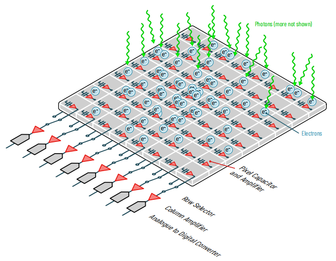
NOTE: The readout process for CMOS cameras differs between 'rolling shutter' and 'global shutter' cameras, as discussed in the text. In either case, each pixel contains a capacitor and amplifier which produce a voltage based on the detected photoelectron count. For each row, the voltages for every column are measured simultaneously by column analogue to digital converters.
Rolling Shutter
1. For a rolling shutter CMOS sensor, starting at the top row (or center for splitsensor cameras), clear the charge from the row to begin that row’s exposure.
2. After the ‘line time’ has elapsed (typically 5-20 μs), move to the next row and repeat from step 1, until the whole sensor is exposing.
3. For each row, charges accumulate during the exposure, until that row has finished its exposure time. The first row to start will finish first.
4. Once exposure is finished for a row, transfer charges to the readout capacitor and amplifier.
5. The voltage in each amplifier in that row is then connected to the column ADC, and the signal measured for every pixel in the row.
6. The readout and reset operation will take the 'line time' to complete, after which the next row to start exposure will have reached the end of its exposure time, and the process repeated from step 4.
7. As soon as the readout is complete for the top row, providing the bottom row has started exposing the current frame, the top row may start the exposure of the next frame (overlap mode). If the exposure time is shorter than the frame time, the top row must wait for the bottom row to start exposure. The shortest possible exposure is typically one line time.
Tucsen’s FL 26BW Cooled CMOS Camera, featuring the Sony IMX533 sensor, uses this rolling shutter technology.
Global Shutter
1. To begin the acquisition, charge is simultaneously cleared from the whole sensor (global reset of the pixel well).
2. Charge accumulates during exposure.
3. At the end of exposure, collected charges are moved to a masked well within each pixel, where they can await readout without new detected photons being counted. Some cameras move charges into the pixel capacitor at this stage.
4. With the detected charges stored in the masked area of each pixel, the active area of the pixel can begin the exposure of the next frame (overlap mode).
5. The process of readout from the masked area proceeds as for rolling shutter sensors: One row at a time, from the top of the sensor, charges are transferred from the masked well to the readout capacitor and amplifier.
6. The voltage in each amplifier in that row is connected to the column ADC, and the signal measured for every pixel in the row.
7. The readout and reset operation will take the ‘line time’ to complete, whereupon the process will repeat for the next row from step 5.
8. Once all rows have been read, the camera is ready to read the next frame, and the process can be repeated from step 2, or step 3 if the exposure time has already elapsed.
Tucsen’s Libra 3412M Mono sCMOS Camera utilizes global shutter technology, enabling clear and rapid capture of moving samples.
Pros and Cons of CMOS Sensors
Pros
● Higher speeds: CMOS sensors are typically 1 to 2 orders of magnitude faster in data throughput than CCD or EMCCD sensors.
● Larger sensors: Faster data throughput enables higher pixel counts and larger fields of view, up to tens or hundreds of megapixels.
● Low noise: Some CMOS sensors can have read noise as low as 0.25e-, rivaling EMCCDs without needing charge multiplication that adds additional noise sources.
● Pixel size flexibility: Consumer and smartphone camera sensors drive pixel sizes down to the ~1 μm range, and scientific cameras up to 11 μm in pixel size are common, and up to 16 μm available.
● Lower power consumption: The low power requirements of CMOS cameras enable them for use in a wider variety of scientific and industrial applications.
● Price and lifetime: Low-end CMOS cameras are typically similar or lower in cost to CCD cameras, and high-end CMOS cameras are much lower in cost than EMCCD cameras. Their expected service lifetime should vastly outstrip that of an EMCCD camera.
Cons
● Rolling shutter: The majority of scientific CMOS cameras have a rolling shutter, which can add complexity to experimental workflows or rule out some applications.
● Higher dark current: Most CMOS cameras have much higher dark current than CCD and EMCCD sensors, sometimes introducing significant noise on long exposures (> 1 second).
Where CMOS Sensors Are Used Today
Thanks to their versatility, CMOS sensors are found in a vast array of applications:
● Consumer Electronics: Smartphones, webcams, DSLRs, action cams.
● Life Sciences: CMOS sensors power microscopy cameras used in fluorescence imaging and medical diagnostics.

● Astronomy: Telescopes and space imaging devices often use scientific CMOS (sCMOS) for high resolution and low noise.
● Industrial Inspection: Automated optical inspection (AOI), robotics, and cameras for semiconductor inspection rely on CMOS sensors for speed and accuracy.
● Automotive: Advanced Driver Assistance Systems (ADAS), rear-view and parking cameras.
● Surveillance & Security: Low-light and motion detection systems.
Their speed and cost-efficiency make CMOS the go-to solution for both high-volume commercial use and specialized scientific work.
Why CMOS Is Now the Modern Standard
The shift from CCD to CMOS didn’t happen overnight, but it was inevitable. Here’s why CMOS is now the imaging industry’s cornerstone:
● Manufacturing Advantage: Built on standard semiconductor fabrication lines, reducing cost and improving scalability.
● Performance Gains: Rolling and global shutter options, improved low-light sensitivity, and higher frame rates.
● Integration & Intelligence: CMOS sensors now support on-chip AI processing, edge computing, and real-time analysis.
● Innovation: Emerging sensor types like stacked CMOS, quanta image sensors, and curved sensors are built on CMOS platforms.
From smartphones to scientific cameras, CMOS has proven to be adaptable, powerful, and future-ready.
Conclusion
CMOS sensors have evolved into the modern standard for most imaging applications, thanks to their balance of performance, efficiency, and cost. Whether capturing everyday memories or conducting high-speed scientific analysis, CMOS technology provides the foundation for today’s visual world.
As innovations like global shutter CMOS and sCMOS continue to expand the technology's capabilities, its dominance is set to continue for years to come.
FAQs
What’s the difference between a rolling shutter and a global shutter?
A rolling shutter reads out image data line by line, which can cause motion artifacts (e.g., skew or wobble) when capturing fast-moving subjects.
A global shutter captures the entire frame simultaneously, eliminating distortion from motion. It’s ideal for high-speed imaging applications like machine vision and scientific experiments.
What is Rolling Shutter CMOS Overlap Mode?
For rolling shutter CMOS cameras, in overlap mode, exposure of the next frame can begin before the current one has fully completed, allowing for higher frame rates. This is possible because each row’s exposure and readout are staggered in time.
This mode is useful in applications where maximum frame rate and throughput are critical, such as in high-speed inspection or real-time tracking. However, it may slightly increase the complexity of timing and synchronization.


