

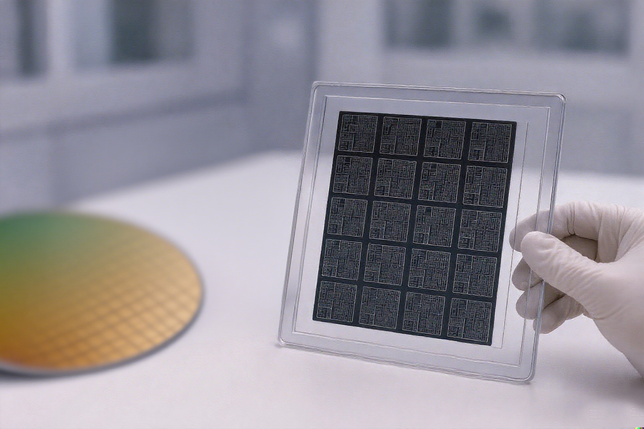
Application Challenges
In photomask inspection, even the slightest defect may be amplified during lithography, compromising the quality of an entire batch of chips. Cameras are thus required to offer extreme resolution and precise contrast reproduction, along with compatibility for deep ultraviolet (DUV) and extreme ultraviolet (EUV) optical imaging to meet the needs of specialized inspection environments. Furthermore, photomask inspection necessitates exceptional stability and long-term consistency to ensure the reliability and reproducibility of results.
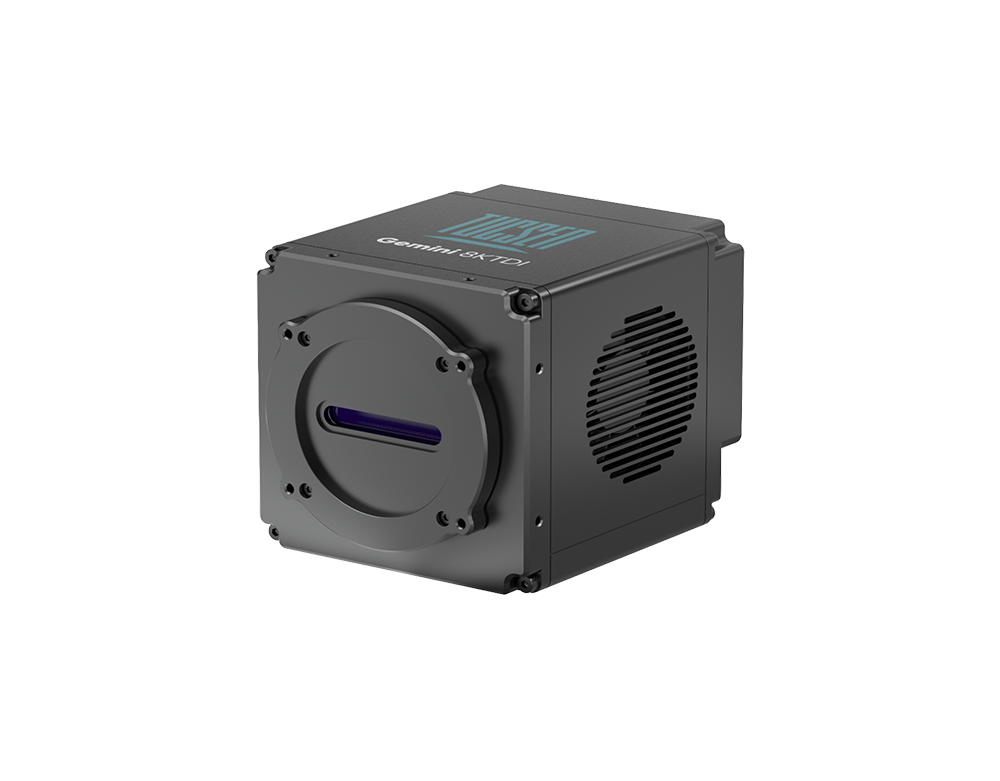
Gemini 8KTDI
Deep Ultraviolet High-Speed TDI-sCMOS Camera
Gemini 8KTDI not only delivers a significant upgrade in sensitivity across its core application wavelengths, with quantum efficiencies of 63.9% at 266 nm and 58% at 355 nm in the UV range, and a peak of 93.4% at 420 nm in the visible range, but also pioneers the implementation of 100G CoF high-speed data interface technology. With an 8K line frequency up to 1 MHz, the overall throughput is doubled compared to the previous generation. Equipped with TUCsen’s stable and reliable cooling and noise reduction system, it effectively suppresses thermal noise during high-speed operation, minimizes data fluctuations, and improves measurement accuracy. This makes it particularly suitable for front-end semiconductor applications demanding both high precision and high throughput.


