
 2026/03/24
In scientific imaging, a pixel is more than a unit of resolution. It is where incoming photons are converted into measurable electrical signal.
Key sensor specifications—such as quantum efficiency (QE), full well capacity, and dynamic range—are rooted in what happens inside each pixel. While these values appear as numbers in a datasheet, they are determined by pixel structure and the way light is converted into charge.
To better understand sensor performance, it is useful to look inside the pixel. This article explores pixel structure, explains how the photodiode converts light into charge, and connects these mechanisms to real imaging performance.
What Is a Pixel in an Image Sensor?
In modern CMOS cameras, a pixel is the basic building block of the image sensor. Pixels are arranged in a two-dimensional array, with each one sampling light from a small region of the scene and contributing to the final image.
In scientific imaging, however, a pixel is more than a geometric sampling unit. It is also where incoming photons are converted into measurable electrical charge, forming the basis of both image formation and signal generation.
Unlike display pixels, which emit light, sensor pixels are designed to detect light with high efficiency and accuracy, even under challenging conditions such as low signal levels or high dynamic range scenes.
Because each pixel generates the signal that defines image quality, its design directly affects light collection efficiency, charge capacity, and the ability to distinguish weak signals from noise. As a result, two sensors with similar pixel size or resolution can still perform differently.
To understand why, we need to examine how a pixel is structured and how it interacts with incoming light.
What Is the Anatomy of a Pixel?
A pixel is not a single light-sensitive point. It is a layered sensing structure made up of optical, electrical, and charge-handling elements that work together to detect light and prepare the signal for measurement.
In a modern image sensor, a photon does not travel directly into a simple detector. Before it can contribute to the image, it may pass through several functional layers designed to guide light, reduce losses, control charge, and support readout. The exact arrangement varies by sensor architecture, but the same basic principle remains: pixel performance depends on how effectively these structures work together.
Source: Pixel cross-section diagram
The Main Structures Inside a Pixel
At a structural level, a pixel can be understood as a combination of optical guidance layers, supporting structures, a sensing region, and isolation features. These elements work together to control how light enters the pixel, how efficiently it reaches the sensing area, and how the resulting signal is preserved.
Optical guidance layers sit at the top of the pixel and help direct incoming photons toward the active region. These typically include a microlens, which concentrates light into the sensing area, as well as a color filter in color sensors. Anti-reflective coatings may also be used to reduce reflection losses as light passes between materials.
Beneath these layers are structural and routing elements, including transparent upper layers and metal wiring. These components are essential for biasing, control, and signal routing, but they also influence how directly light can reach the sensing region.
At the core of the pixel is the light-sensitive silicon, where photon detection begins. When photons are absorbed, they contribute to charge generation, and the resulting electrons accumulate in the pixel well during exposure.
To maintain signal integrity, pixels also include isolation structures, such as trench isolation, which help prevent charge from spreading into neighboring pixels.
What Each Part Does
Each of these structures plays a different role in pixel operation. The microlens improves optical efficiency by directing more incoming light toward the active area. The color filter enables wavelength separation in color imaging, although it also reduces the amount of light available to each pixel compared with a monochrome design. Anti-reflective coatings help preserve signal by minimizing reflection losses at material boundaries.
Metal wiring and associated circuitry are necessary for pixel control and readout, but they occupy space and can limit the openness of the optical path. This is one reason why additional optical guidance, such as microlenses, is so important. The light-sensitive silicon is the region where optical energy begins to turn into electrical signal, while the pixel well serves as the local storage site for the photo-generated charge collected during exposure. Trench isolation helps maintain signal integrity by reducing leakage and crosstalk between neighboring pixels.
Why Pixel Structure Matters
Pixel structure matters because not all of the pixel area contributes equally to light collection and signal formation. The geometry of the optical path, the placement of wiring, the design of the sensing region, and the quality of pixel isolation all influence how efficiently photons are converted into usable signal.
This helps explain why sensor performance cannot be judged by pixel size alone. Two sensors with similar pixel dimensions may still differ in sensitivity, crosstalk behavior, and overall signal quality because the internal structure of each pixel determines how light is guided, absorbed, collected, and preserved.
To understand this more clearly, it helps to follow the path light takes as it travels through the pixel toward the sensing region.
How Does Light Travel Through a Pixel?
To understand pixel performance more clearly, it helps to follow the path a photon takes after arriving at the sensor. Before light can become image data, it must pass through multiple pixel structures that guide, filter, and shape the signal formation process.
In many sensors, the first element the photon encounters is the microlens, which helps steer incoming light toward the active sensing region. In a color sensor, the photon then passes through a color filter that allows only a selected wavelength band to reach that pixel. Anti-reflective coatings may also help reduce reflection losses as light crosses boundaries between different materials.
After passing through these optical layers, the photon may still need to travel through upper structural regions before reaching the sensing silicon. Depending on the pixel architecture, this path can include transparent layers and spaces between metal wiring and other pixel components. The more efficiently light is guided through this path, the greater the chance that it will reach the active region and contribute to usable signal.
Once the photon reaches the light-sensitive silicon, the first stage of detection begins. If the photon is absorbed in the sensing region, its energy can generate charge carriers that contribute to the image signal. These photo-generated electrons are then collected and accumulate in the pixel well during the exposure period.
At this stage, the optical signal has been converted into stored charge, but it is not yet image data. That stored charge must still be measured and converted by the readout chain before it appears as a digital output. This is why the photon’s path through the pixel is so important: every layer it encounters can affect how much signal is ultimately captured and preserved.
The key step in this process takes place in the sensing region itself. To understand how light is converted into electrical charge, we need to look more closely at the role of the photodiode.
What Is a Photodiode and Why Is It the Core of the Pixel?
At the center of every pixel is the photodiode, the structure responsible for converting incoming light into electrical charge. To understand why pixel design affects image sensor performance, it is essential to understand what the photodiode is, how it works, and why it plays such a central role in signal formation.
Source: P-N junction diagram
The Photodiode as the Sensing Core of the Pixel
At the center of the pixel is the photodiode, the light-sensitive structure responsible for converting incoming photons into electrical charge. While other pixel components help guide light, support control, and enable readout, the photodiode performs the first essential step of image formation: detection.
In this sense, the photodiode is the true sensing core of the pixel. It is the region where optical input first becomes a measurable electrical signal, making it fundamental to both image formation and signal generation.
How a Photodiode Converts Light into Charge
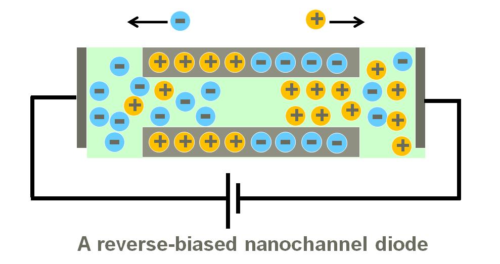
A photodiode is typically formed from a p-n junction in silicon. When operated under reverse bias, this junction creates the electrical conditions needed to separate and collect charge generated by incoming light.
If a photon with sufficient energy is absorbed in the silicon, it can generate an electron-hole pair. Under the internal electric field of the reverse-biased photodiode, these charge carriers are separated: electrons are driven toward the collection region, where they contribute to the signal, while holes move in the opposite direction.
During the exposure period, the photo-generated electrons accumulate and form the basis of the measurable image signal. In this way, the photodiode converts optical input into stored electrical charge that can later be measured by the readout chain.
Why the Photodiode Matters for Pixel Performance
The photodiode matters because it defines how effectively incoming light is turned into usable signal. Its operation directly affects how a pixel responds to light, especially in low-signal imaging conditions where efficient photon-to-electron conversion is critical.
Although the photodiode is only one part of the pixel, it plays a central role in determining signal strength and charge generation. Pixel structure influences how efficiently light reaches the sensing region, while the photodiode determines how that light becomes electrical information.
This is why understanding the photodiode is essential for understanding sensor behavior more broadly. It provides the physical basis for interpreting performance parameters such as sensitivity, quantum efficiency, and full well capacity.
How Pixel Structure and Photodiode Design Affect Sensor Performance?
Pixel structure and photodiode design define how efficiently light is converted into usable signal. Parameters such as sensitivity, quantum efficiency, full well capacity, and signal integrity all depend on how photons reach the sensing region, how they are converted into charge, and how that charge is preserved.
Sensitivity and Quantum Efficiency
Sensitivity depends on how efficiently photons are converted into measurable charge. This is influenced by both the optical path through the pixel and the conversion efficiency of the photodiode.
Pixel structures that guide more light into the sensing region—such as effective microlenses or reduced obstruction from wiring—improve photon collection. The photodiode then determines how many of those photons become electrons, which is reflected in QE.
Fill Factor and Effective Light Collection
Not all of a pixel’s area contributes to light detection. Some space is occupied by wiring and control structures.
The fill factor describes the portion of the pixel that is effectively sensitive to light. Designs that better direct light toward the active region can improve effective light collection, even when pixel size remains the same.
Full Well Capacity and Charge Handling
The full well capacity defines how much charge a pixel can store before saturation. This depends on the design of the photodiode and the charge storage region.
Higher capacity allows the pixel to handle stronger signals without losing detail, which is important for maintaining image information in bright regions.
Crosstalk and Signal Integrity
Crosstalk occurs when charge or optical energy spreads between neighboring pixels. This reduces signal localization and can affect image clarity.
Isolation structures, such as trench isolation, help confine charge within each pixel and improve signal integrity.
Dynamic Range and Weak-Signal Imaging
Dynamic range reflects a sensor’s ability to capture both weak and strong signals. It depends on how efficiently signal is generated, how much charge can be stored, and how well that signal is preserved.
Pixel structure and photodiode design both contribute to this capability, which is critical in applications such as fluorescence imaging and low-light detection.
Why Frontside and Backside Pixel Architectures Behave Differently?
Frontside-illuminated (FSI) and backside-illuminated (BSI) pixels contain the same basic sensing elements, but they differ in how light reaches the photodiode. In FSI designs, photons must pass through wiring and circuitry before reaching the light-sensitive region, while in BSI designs the optical path is more direct.
This difference affects how efficiently photons are delivered to the sensing region, which is why BSI architectures often provide higher quantum efficiency and better low-light sensitivity. For a more detailed comparison of pixel structure, fill factor, and performance tradeoffs, see our article on FSI vs BSI sCMOS Sensors: What’s the Difference.
How Pixel Anatomy Helps You Read a Camera Datasheet?
Understanding pixel anatomy helps interpret camera specifications as connected system behavior rather than isolated numbers. Parameters such as pixel size, quantum efficiency, and full well capacity all reflect how the pixel is structured and how efficiently it converts light into signal.
Pixel Size Is Not the Whole Story
Pixel size is often one of the first specifications users compare, but it should not be treated as a complete indicator of performance. A larger pixel may offer advantages in charge capacity, yet performance also depends on how much of that area is effectively used for light collection and how efficiently light is guided to the active region.
This is why two sensors with similar pixel sizes can still differ in sensitivity and signal quality.
Quantum Efficiency Reflects Both Structure and Conversion
Quantum efficiency is commonly read as a measure of how effectively photons are converted into electrons, but it depends on more than the photodiode alone. Pixel architecture affects how many photons actually reach the sensing region, while the photodiode determines how efficiently absorbed photons become measurable charge.
Reading QE in this context gives a more complete understanding of sensor performance.
Full Well Capacity and Dynamic Range Begin at the Pixel
Full well capacity and dynamic range are often treated as system-level parameters, but their physical basis begins inside the pixel. The photodiode and charge storage region define how much signal can accumulate, while pixel structure influences how efficiently that signal is generated and preserved.
For users evaluating scientific cameras, this makes datasheet comparison more meaningful by connecting specifications to the underlying pixel design rather than viewing each number in isolation.
Conclusion
A pixel is far more than a geometric unit on a sensor. It is a layered structure that guides light, converts photons into charge, and helps preserve signal quality before readout. From microlenses and wiring layers to the photodiode and pixel well, each part of the pixel contributes to how efficiently light becomes usable image data.
Understanding this internal structure makes it easier to interpret specifications such as pixel size, quantum efficiency, full well capacity, and dynamic range in a more meaningful way. For users working with scientific cameras, looking inside the pixel provides a stronger foundation for understanding sensor behavior and evaluating imaging performance in real applications.
Tucsen Photonics Co., Ltd. All rights reserved. When citing, please acknowledge the source: www.tucsen.com


