

 2026/08/26
A semiconductor inspection equipment manufacturer was developing a high-magnification brightfield imaging system for wafer defect inspection.
As wafer structures become increasingly complex, the inspection system needed to identify subtle defects, including low-contrast contamination and defects associated with highly reflective metal structures.
The customer found that conventional industrial cameras could not fully meet the imaging requirements of the application.
The main challenges included:
● Low-contrast defects were difficult to distinguish from the wafer background.
● Limited dynamic range reduced visibility of defects near highly reflective structures.
● Camera noise affected weak defect signal detection.
● Limited software flexibility created challenges for integration with proprietary algorithms.
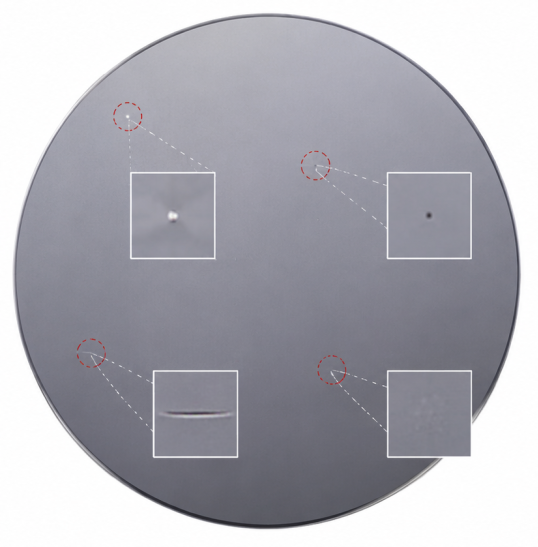
Figure 1. Low-contrast defects
How Did the Dhyana 400BSI V3 Address These Challenges?
The customer integrated the Tucsen Dhyana 400BSI V3 with a 50× high-magnification brightfield microscopy system to evaluate representative wafer defects.
The evaluation focused on:
● Low-contrast contamination defects
● Structural defects associated with metal features
The camera was evaluated for its ability to preserve weak signals while maintaining image details across different intensity levels.
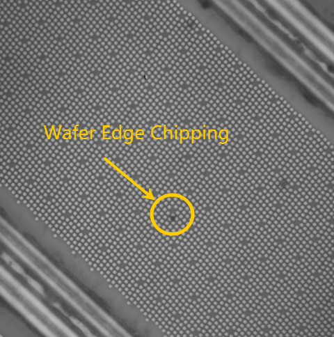
Figure 2. Brightfield wafer inspection using the Dhyana 400BSI V3.
What Results Did the Customer Achieve?
The evaluation demonstrated that the Dhyana 400BSI V3 provided stable and reliable image data for challenging wafer inspection applications.
Low-contrast defects could be clearly distinguished from the background, while details in high-reflectivity metal regions were preserved.
The improved image quality provided better input for the customer's proprietary inspection algorithms and supported further optimization of their automated inspection system.
What Did the Customer Say About the Camera?
“The performance of the Tucsen scientific camera was excellent.”
The customer highlighted the Dhyana 400BSI V3's imaging sensitivity and dynamic range as key advantages during their evaluation. The software's openness was also considered well suited to their algorithm development requirements.
Different Imaging Priorities for Semiconductor Inspection
The results from this evaluation highlight an important trend in semiconductor inspection: image quality is not determined only by resolution or acquisition speed.
For applications where defects are identified through subtle grayscale differences, cameras need to preserve weak signals, maintain dynamic range, and provide consistent image data.
Compared with industrial cameras that typically prioritize resolution, speed, and integration convenience, scientific cameras place greater emphasis on sensitivity, image fidelity, and signal preservation.
|
Imaging Capability |
Industrial Camera |
Scientific Camera |
|
Sensitivity |
★★★ |
★★★★★ |
|
Resolution |
★★★★★ |
★★★ |
|
Speed |
★★★★★ |
★★★ |
|
Background Uniformity |
★★★ |
★★★★★ |
|
Image Data Fidelity |
★★★ |
★★★★★ |
|
Dynamic Range |
★★★ |
★★★★★ |
|
Cooling |
Rarely Equipped |
Standard Configuration |
Figure 3. Different Imaging Priorities of Industrial and Scientific Cameras
For advanced wafer inspection tasks, scientific-grade sCMOS cameras provide the high-quality image data required for defect detection, classification, and quantitative analysis.
More Tucsen Scientific Cameras for Semiconductor Inspection
Tucsen offers a comprehensive range of sCMOS scientific cameras designed to meet diverse semiconductor inspection needs.
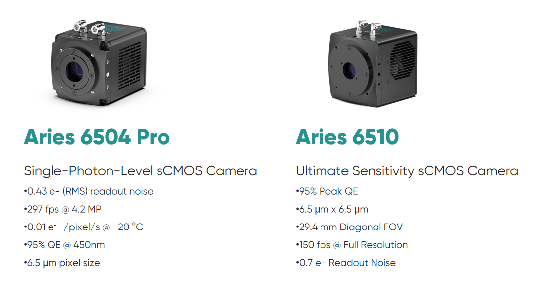
Aries 6504 Pro — Single-Photon-Level Sensitivity for Weak-Signal Inspection
Designed for extremely low-light imaging applications, Aries 6504 is suitable for wafer inspection tasks where detecting weak signals and subtle defects is critical.
Aries 6510 — Large Field of View Imaging for High-Throughput Inspection
With a large sensor format and high imaging performance, Aries 6510 supports large-area wafer inspection systems requiring efficient data acquisition.


