
 2025/07/29
In the fields of bioluminescence high-throughput imaging and industrial high-speed low-light detection, achieving the optimal balance between imaging speed and sensitivity has long been a core bottleneck limiting technological progress. Traditional linear or area array imaging solutions often face difficult trade-offs, making it challenging to maintain both detection efficiency and system performance. As a result, industrial upgrades have been significantly constrained.
The introduction of back-illuminated TDI-sCMOS technology is beginning to address these limitations. This innovative technology not only addresses the physical limitations of high-speed imaging in low-light conditions but also extends its applications beyond life sciences into advanced industrial sectors such as semiconductor inspection and precision manufacturing. With these developments, TDI-sCMOS is becoming increasingly relevant in modern industrial imaging applications.
This article outlines the core principles behind TDI imaging, tracks its evolution, and discusses its growing role in industrial systems.
Understanding Principles of TDI: A Breakthrough in Dynamic Imaging
Time Delay Integration (TDI) is an image acquisition technology based on the line-scanning principle that offers two significant technical features:
Synchronous Dynamic Acquisition
Unlike traditional area cameras that operate on a "stop–shot–move" cycle, TDI sensors continuously expose images while in motion. As the sample moves across the field of view, the TDI sensor synchronizes the pixel columns' motion with the object's speed. This synchronization enables continuous exposure and dynamic charge accumulation of the same object over time, allowing efficient imaging even at high speeds.
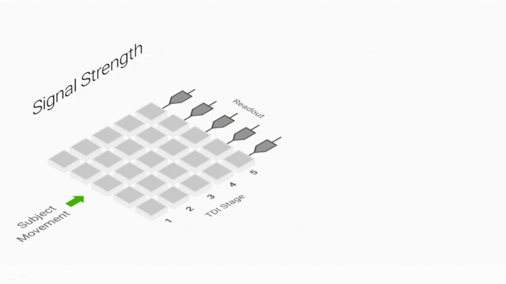
TDI Imaging Demonstration: Coordinated Sample Movement and Charge Integration
Charge Domain Accumulation
Each pixel column converts incoming light into electrical charge, which is then processed through multiple sampling readout stages. This continuous accumulation process effectively enhances the weak signal by a factor of N, where N represents the number of integration levels, improving the signal-to-noise ratio (SNR) under limited lighting conditions.
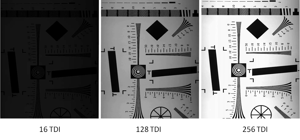
Illustration of Image Quality at Different TDI Stages
Evolution of TDI Technology: From CCD to Back-Illuminated sCMOS
TDI sensors were initially built on CCD or front-illuminated CMOS platforms, but both architectures had limitations when applied to fast and low-light imaging.
TDI-CCD
Back-illuminated TDI-CCD sensors can achieve quantum efficiencies (QE) close to 90%. However, their serial readout architecture restricts imaging speed—line rates typically remain below 100 kHz, with 2K-resolution sensors operating at about 50 kHz.
Front-Illuminated TDI-CMOS
Front-illuminated TDI-CMOS sensors offer faster readout speeds, with 8K-resolution line rates reaching up to 400 kHz. However, structural factors limit their QE, especially in the shorter wavelength range, often keeping it below 60%.
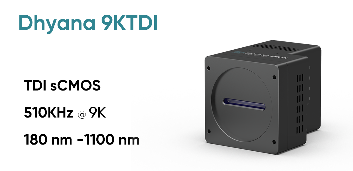
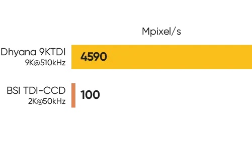
A notable advancement came in 2020 with the release of Tucsen’s Dhyana 9KTDI sCMOS camera, a back-illuminated TDI-sCMOS camera. It marks a significant leap in combining high sensitivity with high-speed TDI performance:
-
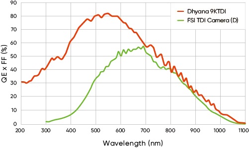
Quantum Efficiency: 82% peak QE—approximately 40% higher than conventional front-illuminated TDI-CMOS sensors, making it ideal for low-light imaging.
-
Line Rate: 510 kHz at 9K resolution, translating to a data throughput of 4.59 gigapixels per second.
This technology was first applied in high-throughput fluorescence scanning, where the camera captured a 2-gigapixel image of a 30 mm × 17 mm fluorescent sample in 10.1 seconds under optimized system conditions, demonstrating substantial gains in imaging speed and detail fidelity over conventional area-scan systems.
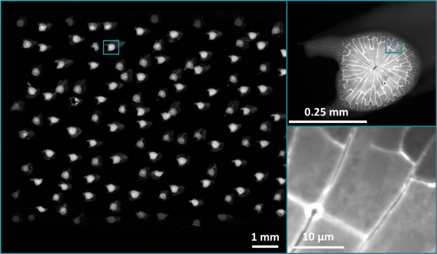
Image: Dhyana 9KTDI with Zaber MVR motorized stage
Objective: 10X Acquisition time: 10.1s Exposure time: 3.6ms
Image size: 30mm x 17mm 58,000 x 34,160 pixels
Key Advantages of TDI Technology
High Sensitivity
TDI sensors accumulate signals over multiple exposures, enhancing low-light performance. With back-illuminated TDI-sCMOS sensors, quantum efficiency above 80% is achievable, which supports demanding tasks such as fluorescence imaging and dark-field inspection.
High-Speed Performance
TDI sensors are designed for high-throughput imaging, capturing fast-moving objects with excellent clarity. By synchronizing pixel readout with object motion, TDI virtually eliminates motion blur and supports conveyor-based inspection, real-time scanning, and other high-throughput scenarios.
Improved Signal-to-Noise Ratio (SNR)
By integrating signals across multiple stages, TDI sensors can produce higher-quality images with less illumination, reducing photobleaching risks in biological samples and minimizing thermal stress in sensitive materials.
Reduced Susceptibility to Ambient Interference
Unlike area-scan systems, TDI sensors are less affected by ambient light or reflections due to their synchronized line-by-line exposure, making them more robust in complex industrial environments.
Application Example: Wafer Inspection
In the semiconductor sector, area-scan sCMOS cameras were commonly used for low-light detection due to their speed and sensitivity. However, these systems can have drawbacks:
-
Limited Field of View: Multiple frames need to be stitched together, resulting in time-consuming processes.
-
Slower Scanning: Each scan requires waiting for the stage to settle before capturing the next image.
-
Stitching Artifacts: Image gaps and inconsistencies affect scan quality.
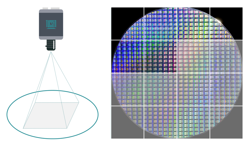
TDI imaging helps address these challenges:
-
Continuous Scanning: TDI supports large, uninterrupted scans without the need for frame stitching.
-
Faster Acquisition: High line rates (up to 1 MHz) eliminate delays between captures.
-
Improved Image Uniformity: TDI’s line-scan method minimizes perspective distortion and ensures geometric accuracy across the entire scan.
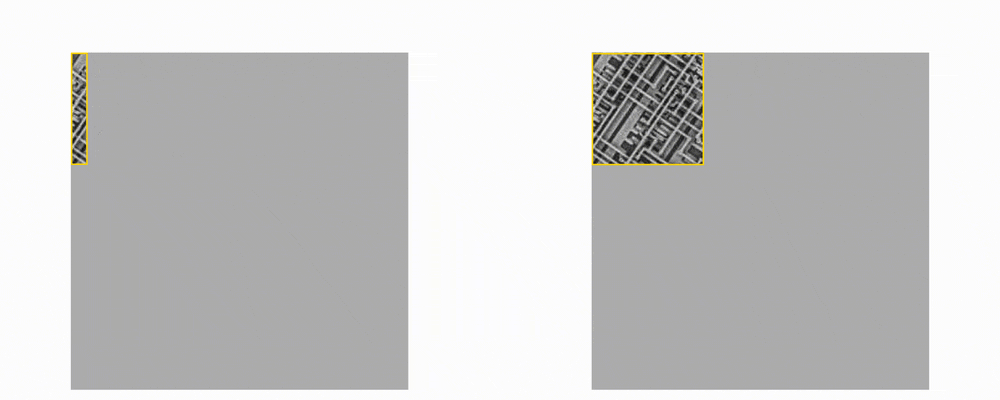
TDI VS Area Scan
Illustration: TDI enables a more continuous and smooth acquisition process
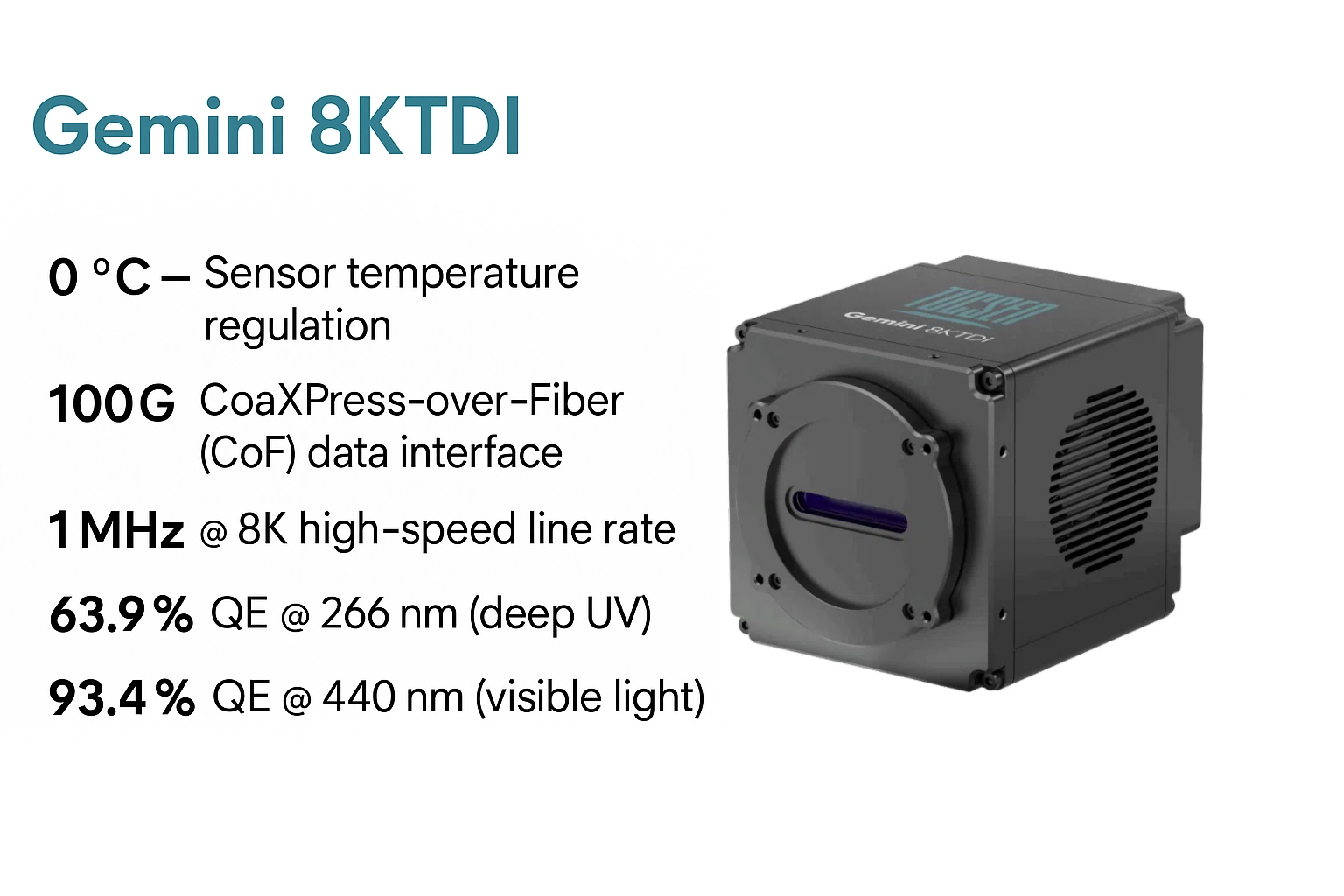
The Tucsen’s Gemini 8KTDI sCMOS camera has been effective in deep ultraviolet wafer inspection. According to Tucsen’s internal testing, the camera achieves 63.9% QE at 266 nm and maintains chip temperature stability at 0°C over extended use—important for UV-sensitive applications.
Expanding Use: From Specialized Imaging to System Integration
TDI is no longer limited to niche applications or benchmark testing. The focus has shifted toward practical integration into industrial systems.
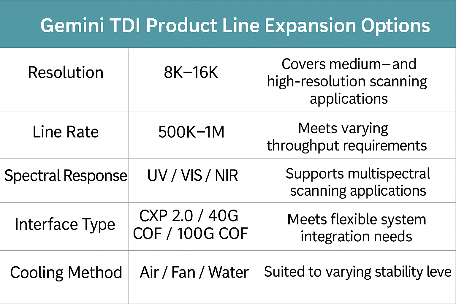
Tucsen’s Gemini TDI series offers two types of solutions:
1. Flagship Models: Designed for advanced use cases like front-end wafer inspection and UV defect detection. These models prioritize high sensitivity, stability, and throughput.
2. Compact Variants: Smaller, air-cooled, and lower power—more suitable for embedded systems. These models include CXP (CoaXPress) high-speed interfaces for streamlined integration.
From high-throughput imaging in life sciences to precision semiconductor inspection, back-illuminated TDI-sCMOS is playing an increasingly important role in enhancing imaging workflows.
FAQs
Q1: How does TDI work?
TDI synchronizes charge transfer across pixel rows with the motion of the object. As the object moves, each row accumulates another exposure, increasing sensitivity, especially in low-light and high-speed applications.
Q2: Where can TDI technology be used?
TDI is ideal for semiconductor inspection, fluorescence scanning, PCB inspection, and other high-resolution, high-speed imaging applications where motion blur and low illumination are concerns.
Q3: What should I consider when choosing a TDI camera for industrial applications?
When selecting a TDI camera, important factors include line rate, quantum efficiency, resolution, spectral response (especially for UV or NIR applications), and thermal stability.
For a detailed explanation on how to calculate line rate, refer to our article:
TDI Series – How to Calculate the Line Frequency of the Camera


