
 2025/10/17
Semiconductors represent the most precise technological achievements in modern industry. As process nodes advance from 7 nm and 5 nm toward 3 nm and beyond, the physical limits of Moore’s Law have pushed optical inspection accuracy to unprecedented challenges.
Ultraviolet (UV) technology—thanks to its shorter wavelengths, higher photon energy, and unique optical properties—has become a core solution for overcoming these precision limits in semiconductor inspection. However, despite the high brightness of UV light sources, the effective photon signal that reaches the detector remains extremely weak after optical transmission and sample scattering. Without highly sensitive imaging methods, many submicron and even nanometer-scale defects would be nearly impossible to identify with accuracy.
This is why high-sensitivity UV cameras serve as the critical link between the light source and the inspection results. They not only determine whether ultra-weak signals can be captured, but also directly affect inspection accuracy and efficiency. In this article, we will systematically analyze the application characteristics and imaging challenges of different UV wavelength bands in semiconductor inspection. Real-world cases will be included to help you select the most suitable UV camera for various inspection scenarios.
Case Studies or Real-World Applications
i) 365 nm: Micron-Level High-Speed Inspection
1. Application Background
The 365 nm wavelength lies within the UVA band (315–400 nm). Its shorter wavelength compared to visible light enables a smaller diffraction limit and higher resolution. Unlike deep UV, 365 nm light sources and optical components are more mature, cost-effective, and efficient. For this reason, 365 nm is widely used in back-end semiconductor packaging and testing for large-area inspection and rapid screening of micron-level defects.
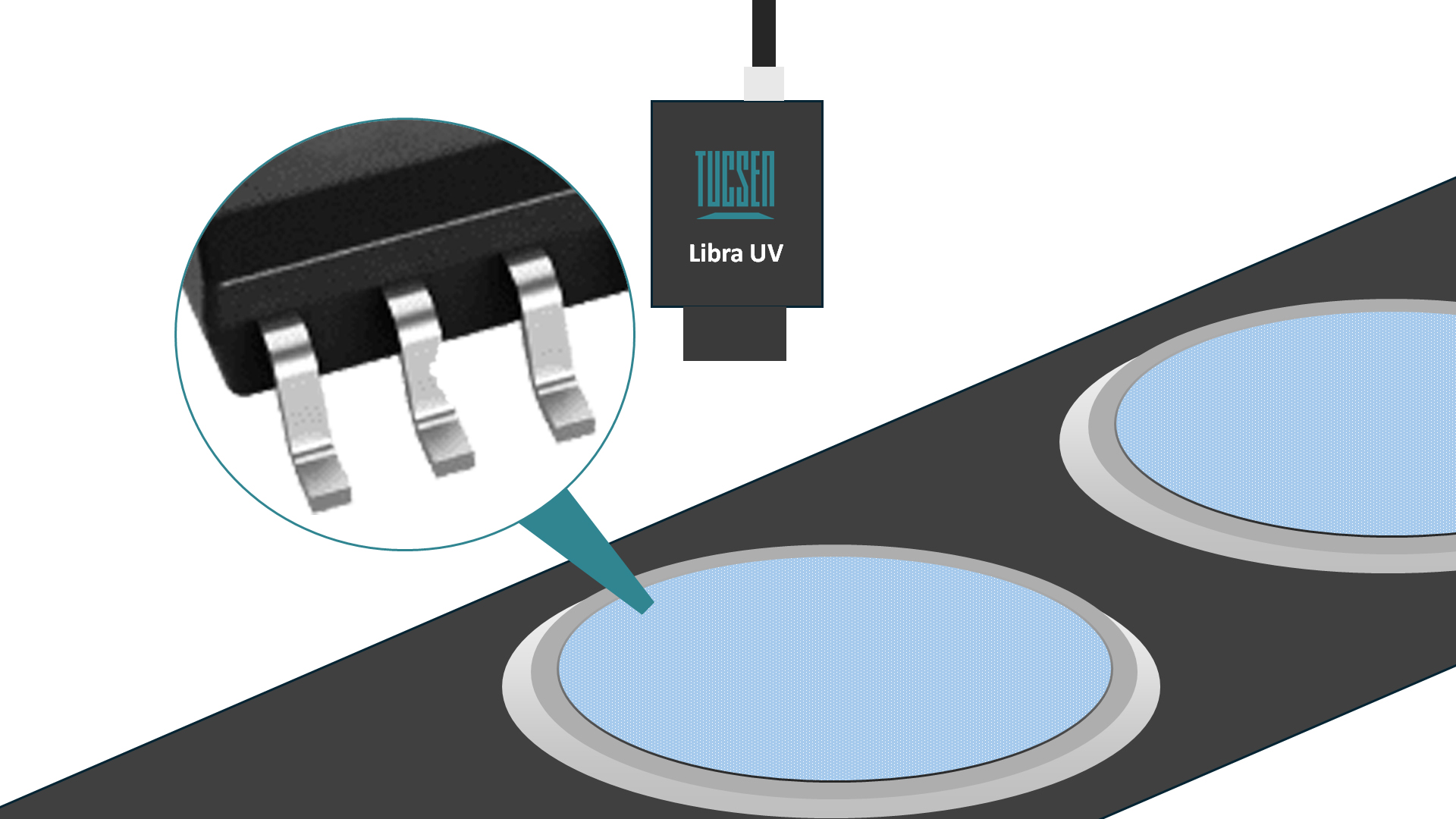
Figure 1-1: Typical Scenarios and Defect Examples in Back-End Semiconductor Packaging and Testing
2. Imaging Challenges
Cameras must combine high UV sensitivity with fast frame rates to meet the requirements of high-speed scanning on production lines. Conventional high-speed industrial cameras typically have limited response in the UV band, with quantum efficiency often below 30%, making it difficult to achieve high signal-to-noise imaging at high frame rates.
3. Recommended Camera
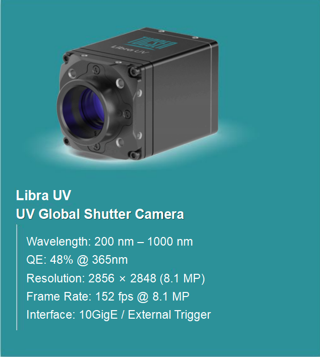
Figure 1-2: UVA Camera Recommendation
Tucsen Libra UV Global Shutter Camera achieves 48% quantum efficiency at 365 nm—placing it among the top performers in UVA cameras and ensuring accurate defect detection. With a high frame rate of 152 fps and a global shutter, it delivers clear images even on fast-moving production platforms, meeting the efficiency demands of high-speed manufacturing lines.
ii) 266 nm: Sub-Micron High-Precision Inspection
1. Application Background
The 266 nm wavelength belongs to the UVC band (100–280 nm), with higher photon energy and shorter wavelength, enabling the detection of sub-micron defects and providing high-contrast imaging. Typical applications include front-end wafer dark-field defect inspection, thin film thickness and uniformity analysis, and photoluminescence experiments.
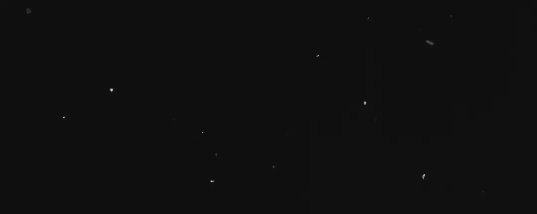
Figure 2-1: Dark-Field Inspection of Semiconductor Wafers (Extremely Weak Scattering Signals)
2. Imaging Challenges
● The target defects are often sub-micron in size, resulting in extremely weak signals that require the camera to have high quantum efficiency (>60%) and low noise performance.
● Due to limitations in silicon-based detector materials, standard sensors often fall short of the sensitivity levels required for professional inspections.
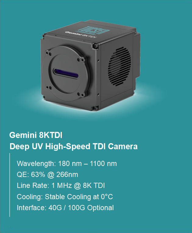
Figure 2-2: UVC Camera Recommendation
Tucsen Gemini 8KTDI sCMOS Camera not only achieves a high UV quantum efficiency of 63.9% at 266 nm, but its TDI (Time Delay Integration) function further enhances the UV imaging signal-to-noise ratio. This minimizes signal attenuation caused by the absorption of deep UV light in the air.
With high-frequency operation (1 MHz at 8K TDI), coupled with Tucsen's stable cooling technology and high-precision DSNU/PRNU correction, the camera not only suppresses thermal noise interference but also provides a more uniform imaging background. This ensures high-speed and high-precision defect analysis for front-end wafer defect inspection.
iii) 193 nm: Key Nodes in Nano-Level Processes
1. Application Background
The 193 nm wavelength is part of the DUV (100–200 nm) deep ultraviolet band and serves as the core light source in photolithography (ArF excimer laser). It plays a crucial role in processes at 20 nm and more advanced nodes. In the inspection phase, 193 nm is widely used for mask defect detection and photoresist pattern verification, revealing sub-micron and even nano-level defects, thereby enabling high-precision process monitoring.
Figure 3-2: Example Images of Dark-Field Defect Inspection in Semiconductors
2. Imaging Challenges
● 193 nm light is strongly absorbed by oxygen and water vapor in the air, leading to significant signal attenuation. Applications requiring longer optical paths may even necessitate a vacuum or inert gas environment.
● Conventional silicon-based detectors have limited response to high-energy 193 nm photons. Typically, back-illuminated (BSI) chips are needed, often accompanied by special optimization processes to enhance quantum efficiency.
● To ensure high signal-to-noise ratio imaging under weak signal conditions and stable long-term operation, cameras must incorporate deep cooling and low-noise design.
3. Recommended Camera
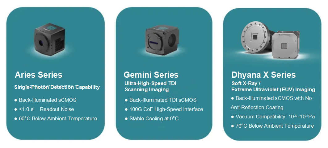
Figure 3-3: Recommended DUV/EUV Cameras
Technical Challenges and Solutions for UV Imaging in Semiconductors
Technical Challenges in UV Imaging
1. Signal Attenuation
UV light, particularly at shorter wavelengths, is highly susceptible to attenuation as it passes through the air. This attenuation occurs due to the absorption by water vapor and oxygen in the atmosphere, which weakens the signal and reduces detection capabilities. In semiconductor inspection, where the defects being identified are often sub-micron or nano-scale, this signal loss can drastically impact imaging accuracy.
2. Sensor Sensitivity
Conventional silicon-based sensors often struggle to provide sufficient sensitivity for high-energy UV light, particularly at wavelengths like 193 nm and 266 nm. As a result, the need for specialized back-illuminated (BSI) chips and optimized optical systems becomes essential. Without these advancements, achieving high quantum efficiency and low noise in UV imaging is nearly impossible.
3. Thermal and Environmental Noise
As UV imaging systems operate under low-light conditions, even slight environmental changes or thermal noise from the camera can drastically reduce the quality of the captured images. High-end UV cameras are required to incorporate advanced cooling systems and low-noise designs to ensure optimal performance in semiconductor production environments.
Solutions for Overcoming Challenges
● Vacuum or Inert Gas Environments
To counteract signal attenuation from atmospheric absorption, semiconductor inspection processes utilizing UV light at wavelengths such as 193 nm are often performed in vacuum or inert gas environments. This minimizes the impact of air on signal quality.
● Back-Illuminated Sensors (BSI)
BSI sensors are specifically designed to enhance the sensitivity of UV cameras, allowing them to respond more effectively to higher energy UV light. These sensors help improve quantum efficiency and enable more accurate imaging of defects at smaller wavelengths.
● Advanced Cooling and Low-Noise Designs
To mitigate thermal noise, advanced cooling solutions (like Peltier cooling) are integrated into high-performance UV cameras. This ensures stable and reliable long-term operation while maintaining a low-noise level for high-quality imaging.
Factors to Consider When Choosing a UV Camera
Selecting the right UV camera for semiconductor inspection involves more than just picking the one with the highest resolution. Here are some key factors to consider:
1. Quantum Efficiency (QE)
Quantum efficiency measures how effectively a camera sensor converts incoming UV photons into useful electrical signals. A higher QE means better sensitivity and signal capture, particularly crucial in semiconductor inspections where defects are often sub-micron or nano-scale.
2. Noise Performance
Noise, both thermal and electronic, can interfere with the imaging process, especially when dealing with weak UV signals. Choosing a UV camera with low noise is critical to achieving clear, high-quality images that accurately represent defects.
3. Wavelength Range
Different wavelengths are better suited to different types of defects and applications. Cameras with specific wavelength capabilities (365 nm, 266 nm, 193 nm) should be selected based on the target semiconductor process. Understanding the wavelength's interaction with the material being inspected helps maximize defect detection.
4. Cooling Systems
In high-performance UV cameras, especially those used in industrial environments, advanced cooling systems are essential to reduce thermal noise and ensure stable operation during long periods of use.
5. Frame Rate
High-speed semiconductor manufacturing lines require high frame rates to capture fast-moving defects. Choosing a UV camera with an optimal frame rate (such as 152 fps at 365 nm) ensures that the camera can keep up with fast inspection cycles without sacrificing image quality.
6. Integration with Existing Equipment
A UV camera must seamlessly integrate with the existing semiconductor inspection and manufacturing systems. Consider factors such as data interface bandwidth, synchronization capabilities with upstream and downstream equipment, and compatibility with current optical systems.
Comparison of UV Imaging Technologies vs. Other Techniques
UV imaging provides several advantages over traditional inspection methods, but it also comes with its own set of challenges. Here's a comparison with other common technologies:
1. UV Imaging vs. Optical Inspection
Optical inspection methods often rely on visible light, which is limited by diffraction, making them unsuitable for detecting sub-micron and nano-level defects. UV imaging, on the other hand, offers shorter wavelengths, enabling higher resolution and the ability to identify smaller defects with greater precision.
2. UV Imaging vs. Electron Microscopy (EM)
While electron microscopy offers highly detailed images, it is typically slower and more expensive. UV imaging provides a quicker and more cost-effective solution for high-speed production lines, while still offering adequate resolution for most semiconductor defects.
3. UV Imaging vs. X-ray Inspection
X-ray inspection is useful for identifying internal defects but is limited in detecting surface anomalies, especially on thin layers or materials that do not effectively interact with X-rays. UV imaging excels in surface defect detection and is more suited for semiconductor process monitoring, such as mask inspection.
Summary of UV Camera Selection Strategy
From UVA to EUV, as the UV wavelength shortens, the inspection difficulty increases, along with the higher performance demands placed on cameras. Cameras must feature higher quantum efficiency (QE), lower noise levels, and superior system stability to maintain clear and reliable imaging under extremely weak signal conditions. As one of the few providers in China offering UV camera solutions covering the full range from UVA to EUV, Tucsen can match you with high-reliability products and performance guarantees for various inspection stages.
In semiconductor manufacturing and inspection, camera selection must not only match the UV wavelength but also comprehensively consider factors such as optical systems, spectral response, platform scanning speed, data interface bandwidth, and synchronization with upstream and downstream equipment. If you plan to deploy UV imaging solutions in your equipment system, feel free to contact us. Our technical team will provide full-process technical support, from camera selection to system implementation, tailored to your application needs.
Tucsen Photonics Co., Ltd. All rights reserved. When citing, please acknowledge the source: www.tucsen.com


